
Upgraded EMC Material Requirements in Advanced Packaging
Advanced packaging has changed the way semiconductor systems are built, and with that change has come a quieter but equally important evolution in materials. One of the most overlooked heroes in the entire stack is EMC, or epoxy molding compound. In simple packages, EMC was mostly a protective shell. In advanced packaging and heterogeneous integration, it has become a structural, thermal, mechanical, and reliability-critical material that helps make the whole system viable.
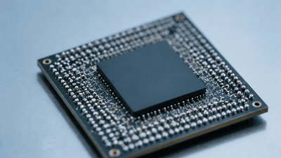
That shift is why EMC material requirements are being upgraded so rapidly. The package is no longer just a container for a single die. It is a dense assembly of multiple dies, interposers, redistribution layers, high-bandwidth memory, and sometimes stacked 3D structures. EMC has to survive more heat, manage more stress, coexist with finer interconnects, and support more complex assembly flows than ever before. It has gone from background material to active enabler.
Why EMC Matters More Now
At first glance, EMC might seem like a supporting character. Its job is to encapsulate the die, protect it from moisture and contamination, and give the package mechanical strength. But in advanced packaging, those functions become much harder because the package itself is more complex and more fragile. A modern multi-die module may contain very thin dies, stacked memory, chiplets with different thermal behaviors, and fine-pitch interconnects that cannot tolerate much mechanical distortion.
This means EMC must do several things at once. It has to provide protection without damaging delicate structures. It has to support thermal cycling without cracking or delaminating. It has to maintain low warpage while accommodating large, heterogeneous package footprints. And it has to remain compatible with increasingly demanding process conditions, including high-temperature assembly, fine-pitch molding, and post-mold reliability requirements.
That is a much taller order than in legacy packages. As a result, the material science behind EMC is becoming just as important as the silicon architecture itself.
What Changed in Advanced Packaging

The biggest reason EMC requirements are being upgraded is that packages themselves have changed. Traditional single-die packages were relatively forgiving. Even if the mold compound was not perfect, there was enough margin in the design to absorb small mismatches or stress concentrations. Advanced packaging removes much of that margin.
Consider the environments EMC now has to support:
- 2.5D packages with large interposers and multiple HBM stacks.
- Fan-out wafer-level or panel-level packages with very fine redistribution layers.
- 3D integration with stacked dies, hybrid bonding, or TSV-based structures.
- High-density system-in-package modules for mobile, automotive, networking, and AI.
In each of these cases, EMC is expected to participate in a much more delicate balancing act. It must keep the structure rigid enough for assembly and handling, but flexible enough not to create destructive stress. It must resist moisture, support long lifetimes, and avoid interfering with electrical performance in dense layouts. That is why “standard EMC” is no longer enough for many advanced packages.
Mechanical Stability Becomes a Priority
One of the most important upgraded requirements is mechanical stability. Advanced packages often contain dies of different sizes, thicknesses, and materials, and those differences create warpage risk. When the package heats and cools, the various materials expand and contract at different rates. If the EMC is not carefully engineered, it can amplify that stress rather than relieve it.
This is especially critical in large AI and HPC packages, where the package footprint is substantial and the interconnect density is extreme. Even slight warpage can disrupt alignment, affect solder joint reliability, or reduce yield during assembly. EMC formulations therefore need better modulus control, lower shrinkage during cure, and a coefficient of thermal expansion that works in harmony with substrates, dies, and interposers.
In practice, this means materials engineers are tuning EMC not just for protection, but for package-level mechanics. The goal is no longer simply to “seal” the chip. It is to help the entire structure stay flat, stable, and predictable across processing and operation.
Thermal Demands Are Rising Fast
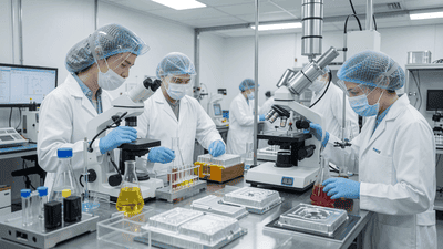
Advanced packaging is also putting much more pressure on EMC from a thermal standpoint. As more computation is packed into less area, power density rises. That is especially true in AI accelerators, where multiple dies and HBM stacks can generate intense local hotspots. EMC sits close to these heat sources, and while it is not the primary heat path, its thermal behavior still matters.
The upgraded requirement here is subtle but important: EMC must tolerate higher temperatures without degrading, softening excessively, or producing reliability problems over time. It also needs to maintain stable mechanical behavior at elevated temperatures so that the rest of the package does not drift or warp under load.
For some package types, EMC also interacts indirectly with thermal management strategies. If the mold compound expands too much or conducts heat poorly in the wrong direction, it can complicate lid design, heat spreader integration, or underfill behavior. This makes thermal performance part of the EMC selection process, not an afterthought.
Electrical Integrity and Miniaturization
EMC has traditionally been thought of as electrically inert, but that assumption is becoming less comfortable in advanced packaging. As interconnects get denser and packages get smaller, parasitic effects matter more. The mold compound’s dielectric properties, contamination behavior, and interaction with nearby structures can all influence package performance.
This is especially true in fan-out packages and high-frequency modules. When signal paths are short and tightly packed, even modest variations in dielectric constant or loss tangent can affect high-speed performance. EMC therefore needs tighter control over composition and more predictable behavior across batches.
Miniaturization also raises a manufacturing issue: thinner packages and finer features make the mold process more sensitive. Voids, delamination, resin bleed, and surface nonuniformity become harder to tolerate. In advanced packaging, EMC is no longer just a filler around the die. It becomes part of the precision environment in which the package is built.
Moisture Resistance and Reliability
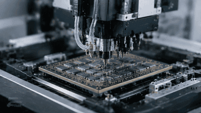
Moisture is a silent enemy in semiconductor packaging. It can lead to delamination, corrosion, popcorning, and long-term reliability failures. As heterogeneous integration becomes more complex, these risks only increase because there are more interfaces, more materials, and more potential failure points.
Upgraded EMC materials must therefore offer stronger moisture resistance and better long-term adhesion. They must survive storage, reflow, thermal cycling, and field operation without compromising the integrity of the package. This is particularly important in automotive, industrial, and infrastructure applications where reliability expectations are very high and service life can stretch over many years.
In some advanced packages, EMC must also coexist with sensitive components such as MEMS, optics, or RF structures. In those cases, moisture control is not just about mechanical survival. It is about preserving performance and stability in systems that are far more sensitive than older package generations.
Compatibility with Diverse Materials
Heterogeneous integration means the package can contain many different materials and structures. Silicon dies, compound semiconductors, organic substrates, redistribution layers, interposers, underfills, lids, and thermal materials may all live together in the same system. EMC has to be compatible with all of them.
That compatibility is one of the hardest material challenges in advanced packaging. A compound that works beautifully with silicon might perform poorly with copper-rich structures or low-k dielectrics. A formulation that cures well in one package geometry might produce unacceptable stress in another. EMC design is therefore becoming increasingly application-specific.
This is why one size no longer fits all. Package developers now need EMCs tailored to:
- Low-warpage fan-out packages.
- High-temperature automotive modules.
- Large AI packages with wide footprints and intense thermal cycling.
- Fine-pitch 3D structures that need very stable mechanical support.
The more diverse the package, the more carefully the EMC has to be selected and tuned. Material compatibility has become one of the core design constraints in advanced encapsulation.
Processability and Manufacturing Windows
A good EMC is not only about final properties. It also has to behave well during manufacturing. That means it must flow, cure, fill, and release in ways that are compatible with modern packaging lines. In advanced packaging, the process window is often tight, because the die and interconnect structures are delicate and expensive.
For example, if the EMC flows too aggressively, it can displace fine structures or create voids. If it cures too fast or shrinks too much, it can distort the package. If it is too brittle after cure, it may crack under thermal stress. And if it requires an overly narrow process window, production yield can suffer.
This is why upgraded EMC requirements now include not only material performance but also process robustness. Manufacturers want compounds that support:
- Predictable viscosity and flow behavior.
- Controlled cure kinetics.
- Low voiding and good cavity fill.
- Stable performance across different package sizes and geometries.
In other words, the ideal EMC is a material that behaves nicely in the factory and stays stable in the field.
Advanced Packaging Needs Material Co-Design
One of the clearest lessons from heterogeneous integration is that materials can no longer be chosen in isolation. EMC must be co-designed with the rest of the package stack. That means package architects, materials scientists, mechanical engineers, and process teams need to work together much earlier than before.
Why? Because changing the EMC can affect:
- Warpage and alignment during assembly.
- Stress on die edges, solder joints, and micro-bumps.
- Heat flow through the package.
- Moisture reliability and delamination risk.
- Final package thickness and mechanical response.
A package that looks excellent on paper can still fail if the EMC choice is wrong. That is especially true in multi-die systems where different materials interact in complex ways. The best advanced packaging teams now treat EMC as a design variable, not a commodity.
What This Means for the Supply Chain
The rising demands on EMC are also affecting the materials supply chain. Suppliers are being asked for more tailored formulations, tighter consistency, and faster support for new package types. That means more collaboration with foundries, OSATs, and device makers, and more pressure to qualify new compounds quickly without sacrificing reliability.
For customers, this can be a blessing and a headache. On the one hand, better EMC options allow more ambitious package designs. On the other hand, qualification cycles become longer and more expensive, especially when a package needs a unique EMC to satisfy thermal, mechanical, or environmental requirements. In advanced packaging, materials selection is becoming a strategic procurement issue as much as a technical one.
The supply chain is also moving toward regional diversification. As advanced packaging expands in different geographies, local EMC development and qualification become more important. This adds resilience, but it also raises the bar for new entrants who must prove not only performance but process stability and long-term reliability.
Future Directions
The next wave of EMC development will likely focus on specialization. We are likely to see formulations optimized for different advanced packaging categories rather than one general-purpose compound. Some future directions may include:
- Lower-stress EMCs for large AI packages with extreme warpage sensitivity.
- High-thermal-stability compounds for automotive and industrial modules.
- Low-loss EMCs for high-frequency and RF-sensitive packages.
- Materials with improved compatibility for fan-out, 3D stacking, and hybrid bonding environments.
There may also be more interest in EMCs that integrate better with thermal solutions, such as heat spreaders, liquid cooling structures, or embedded thermal paths. As advanced packaging continues to move toward higher density and more aggressive integration, the mold compound may need to become smarter, not just tougher.
Conclusion
Upgraded EMC requirements are a clear sign that advanced packaging has matured into a true system-level discipline. The mold compound is no longer just a protective shell. It is a critical material that affects mechanical stability, thermal behavior, moisture reliability, process yield, and package performance. In heterogeneous integration, where many different dies and materials must coexist in one compact system, EMC has become one of the quietest but most important enablers.
The lesson is simple: as packages become more complex, the materials inside them must become more capable. EMC is evolving to meet that challenge, and the companies that understand this early will be better positioned to build the next generation of high-performance, reliable, and manufacturable advanced packages. In the end, the future of heterogeneous integration will not be determined by silicon alone. It will also depend on the materials that hold everything together.





